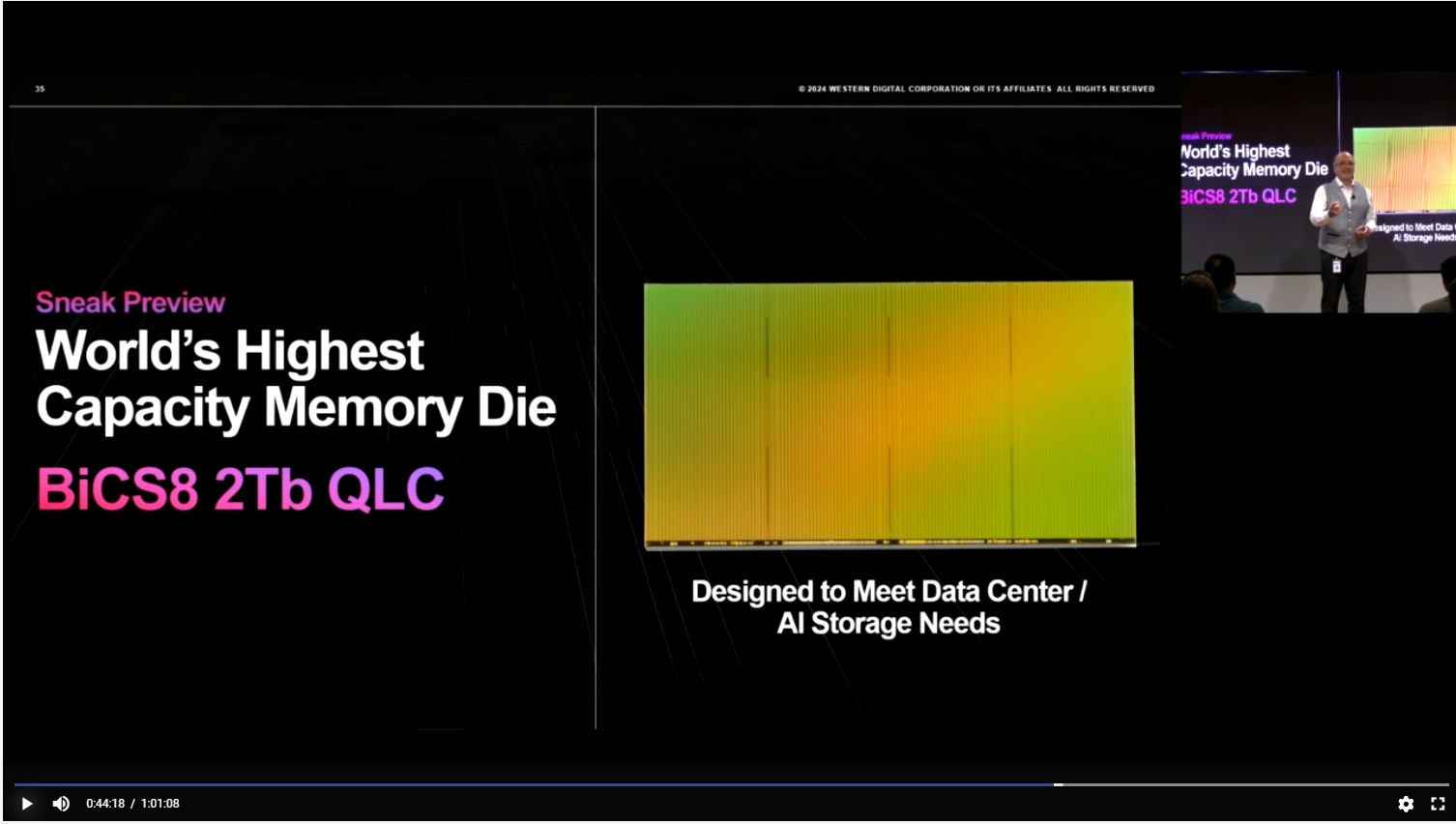
In a rather unexpected turn of events, Western Digital (WD) has teased the industry’s first 2Tb 3D QLC NAND device at an investor conference ahead of its official announcement. The new flash memory could potentially reshape the high-capacity solid-state drives market, enabling much faster and larger SSDs that consume less power. The device uses the proven218-layer BiCS8 production nodeand is so tiny it can fit on a fingertip. WD also shared plenty of comparative performance data, touting power, density, and I/O performance gains over competing flash.
“I am really excited to share with you a preview of the BiCS8 2Tb 3D QLC die,“saidRobert Soderbery, Executive Vice President and General Manager of Western Digital’s Flash Business. “We have designed this die to meet the data center and AI storage needs. We are going to shortly announce this product, but I want to share it with you today. This happens to be the world’s highest-capacity memory die.”
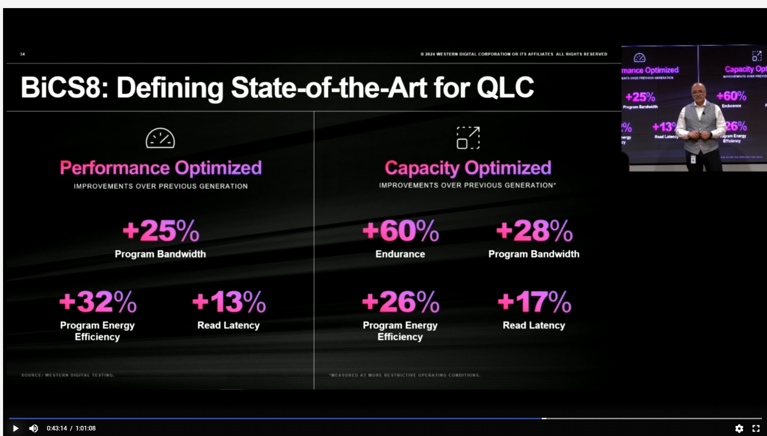
A 2Tb (256GB) 3D QLC NAND die is indeed a huge achievement, as the ‘base’ product that Western Digital introduced on its 218-layer BiCS8 production technology is a 1Tb 3D TLC device. At this point, we have no idea about the exact architecture of the 2Tb IC, such as the speed of its interface (it is probably fast), or the number of planes, or its latency. However, the company did share detailed comparative performance and power metrics (below), and given the fact that the company positions the device for data centers in general and AI storage needs in particular, one can make some assumptions about its performance targets.
Now, a 256GB 3D QLC NAND device would allow manufacturers to build a 1TB SSD using just four memory ICs and a 2TB drive using eight devices, which greatly lowers their costs. Creating a 16-die package would enable a stunning 4TB in a single chip package.
Thus, assuming that Western Digital (and its manufacturing partner Kioxia) can produce these 2Tb 3D QLC NAND ICs in high volume and with decent yields, the new device can redefine the cost of high-capacity solid-state drives.
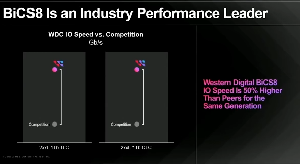
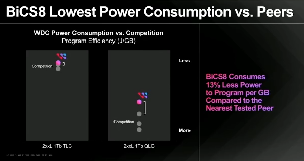
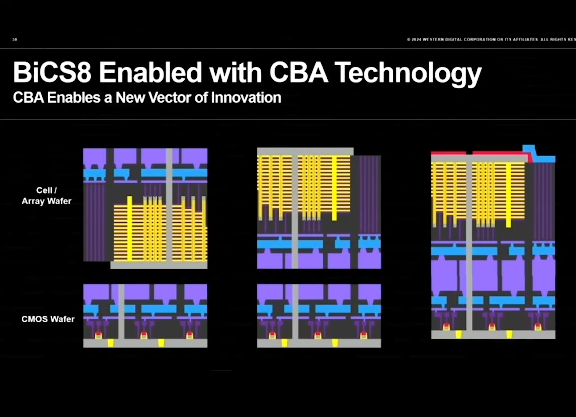
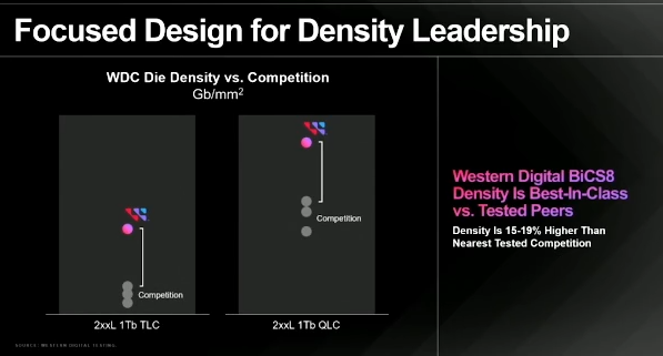
As you can see in the album above, WD says its QLC die density is 15 to 19% denser than the competition. It also claims to be 50% faster than competing NAND (I/O speed) while requiring 13% less power to program per gigabyte of data than competitors. You can also see the method the company uses to create the die — WD creates a die with only the CMOS control circuitry and another with the stacked memory cells, then flips the latter over and bonds the two devices together using hybrid bonding technology (much like Chinese fabYMTC’s Xtacking tech).
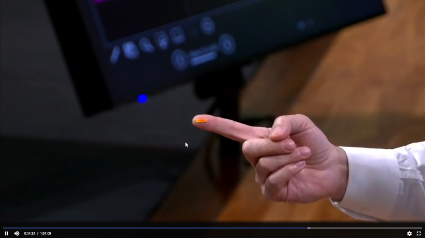
“We typically show you a wafer, but I felt like the view of a wafer does not quite convey what we have achieved,” said Sodebery. “So, if you allow me for a quick second, I want to show you the die. I have one here. Please zoom in [on] what I am holding on my finger here. This is the size of the die, much smaller than my fingertip.”
Get Tom’s Hardware’s best news and in-depth reviews, straight to your inbox.
Western Digital plans to formally announce its 2Tb 3D QLC NAND device soon, so we’ll likely learn more detailed specifications soon.
Anton Shilov is a contributing writer at Tom’s Hardware. Over the past couple of decades, he has covered everything from CPUs and GPUs to supercomputers and from modern process technologies and latest fab tools to high-tech industry trends.