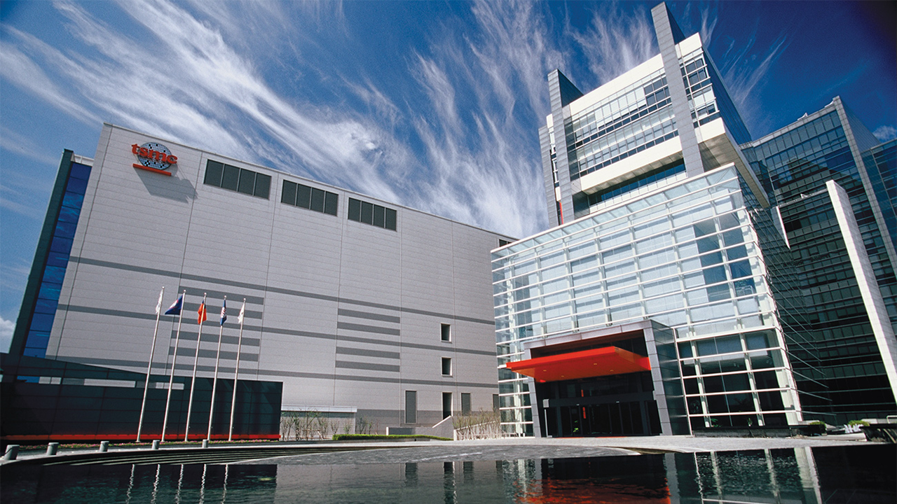
The U.S. government hasshed some lighton TSMC’s plans concerning the new Fab 21 complex near Phoenix, Arizona, and revealed the foundry’s plans to eventually build chips on its A16 (1.6nm-class) and N2 (2nm-class) process technologies in America by the end of the decade. Also, TSMC and the U.S. government today finalized funding of TSMC’s Fab 21 under theU.S. CHIPS and Science Act.
TSMC and the U.S. Department of Commerce finalized the deal under which the contract chipmaker gets $6.6 billion in direct funding and $5 billion in loan guarantees under the CHIPS and Science Act to build its Fab 21 site in Arizona. The whole campus will require funding of approximately $65 billion, includes three fab modules, and will be completely built by the end of the decade. The fabs will create over 6,000 direct manufacturing jobs and over 20,000 accumulated construction jobs.
While the formal sign-off of the agreement between TSMC and the Commerce Department is important, the preliminary roadmap outline for Fab 21 is definitely no less so. For now, TSMC is committed to make chips on its most advanced production node announced to date — A16 — in the U.S., albeit at least about three years after it enters mass production in late 2026 in Taiwan.
TSMC’s 1.6nm process, like its 2nm counterparts (N2, N2P, N2X), uses gate-all-around (GAA) nanosheet transistors and adds a unique backside power delivery system dubbed Super Power Rail. This advancement boosts performance and efficiency over N2P, offering up to 10% higher clock speeds at the same voltage and 15%–20% lower power consumption at the same frequency and complexity. Also, it promises a 7%–10% increase in transistor density, depending on design.

“TSMC appreciates the continual collaboration with customers, partners, local communities and the U.S. government beginning in early 2020,” said Dr. C.C. Wei, chairman and chief executive of TSMC. “The signing of this agreement helps us to accelerate the development of the most advanced semiconductor manufacturing technology available in the U.S.”
TheFab 21 manufacturing sitewill house three fab modules each producing chips using various process technologies, as per agreement between TSMC and the U.S. Department of Commerce:
The CHIPS Program Office (CPO) will release direct funding to TSMC Arizona for project capital expenses as construction, production, and commercial milestones are reached, while loans will be provided for amounts invested in these capital expenditures.
Get Tom’s Hardware’s best news and in-depth reviews, straight to your inbox.
“Today’s final agreement with TSMC — the world’s leading manufacturer of advanced semiconductors — will spur $65 billion dollars of private investment to build three state-of-the-art facilities in Arizona and create tens of thousands of jobs by the end of the decade,” said President Joe Biden. “This is the largest foreign direct investment in a greenfield project in the history of the United States. The first of TSMC’s three facilities is on track to fully open early next year […]. Today’s announcement is among the most critical milestones yet in the implementation of the bipartisan CHIPS & Science Act, and demonstrates how we are ensuring that the progress made to date will continue to unfold in the coming years, benefitting communities all across the country.”
Anton Shilov is a contributing writer at Tom’s Hardware. Over the past couple of decades, he has covered everything from CPUs and GPUs to supercomputers and from modern process technologies and latest fab tools to high-tech industry trends.
