TSMC is developing a new advanced chip packaging method using rectangular panel-like substrates to meet growing demand for advanced multi-chiplet processors, reportsNikkei. The development is still in its early stages and could take several years to commercialize, but if it occurs, it will represent a significant technical change for the world’s largest contract chipmaker.
Instead of300mm diameter wafers, TSMC’s new method reportedly uses rectangular substrates measuring 510mm by 515mm. These panels offer a usable area approximately 3.7x larger than traditional 300-mm round wafers, allowing more chips to be produced per wafer and reducing waste at the edges. However, the new method requires brand-new equipment, which means that TSMC will not be able to use traditional fab tools. The report says that TSMC is currently working with equipment and material suppliers on this new packaging technology but does not go into details.
“[TSMC]closely monitors progress and development in advanced packaging, including panel-level packaging,” a statement by TSMC published by Nikkei reads.
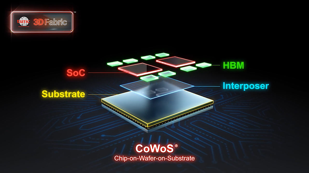
The company’s current advanced chip packaging techniques, such as CoWoS (chip-on-wafer-on-substrate), use 300-mm silicon wafers and are crucial for producing AI processors for clients like Nvidia, AMD,Amazon, andGoogle. However, as AI chips grow in size and complexity, the efficiency of these methods may decline, prompting the need for the new rectangular substrates, Nikkei says.

Transitioning to rectangular substrates is technically challenging and requires significant changes to production tools and materials. The precision needed for chip production is higher than that for display and PCB manufacturing, making this shift complex.
This transition to rectangular substrates is considered a long-term plan, likely taking five to ten years. Significant overhauls of facilities, including upgrades to robotic arms and automated material handling systems, will be necessary to accommodate the new substrate shapes and ensure the success of this advanced packaging method.
TSMC’s deep pockets and industry influence are critical in pushing equipment makers to adapt, but it remains to be seen whether the plan will ever come to fruition.
Get Tom’s Hardware’s best news and in-depth reviews, straight to your inbox.
Other industry players, including Intel and Samsung, are also exploring panel-level packaging, according to Nikkei Companies like Powertech Technology and display panel makers such as BOE Technology and Taiwan’s Innolux are reportedly investing in this technology to diversify into the semiconductor industry.
Anton Shilov is a contributing writer at Tom’s Hardware. Over the past couple of decades, he has covered everything from CPUs and GPUs to supercomputers and from modern process technologies and latest fab tools to high-tech industry trends.
