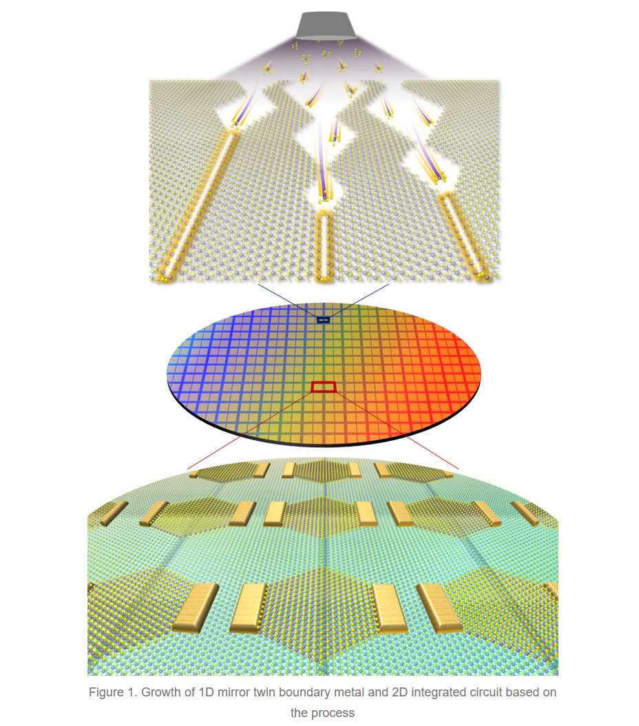
Korean researchers have developed a method togrow sub-nanometer semiconductorlogic circuits. The team from the Institute for Basic Science (IBS) claims that they grew 1D metallic materials with a width of less than 1nm and developed them into 2D circuits. In effect, the 1D metals acted as a gate electrode of an ultra-miniaturized 2D transistor.
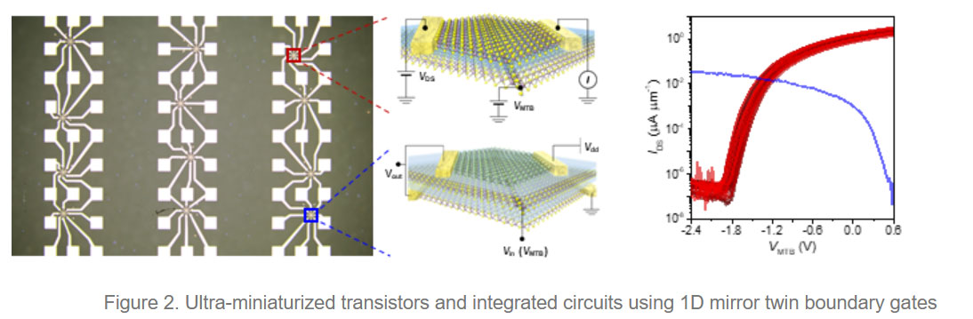
The headlining technology could be very important, as it exceeds predictions outlined on the International Roadmap for Devices and Systems (IRDS) by the IEEE. While the IEEE predicted semiconductor node technology to reach around 0.5 nm by 2037 with transistor lengths of 12nm, the IBS researchers demonstrated a 1D MTB (mirror twin boundary) gate can be as small as 3.9nm.
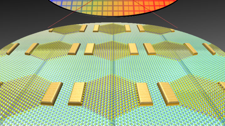
It goes almost without question that creating ultra-miniaturized transistor devices based on2D semiconductorscomes with significant technical challenges. The scientists note that in traditional semiconductor fabrication processes, reducing the gate length below a few nanometers is limited bylithography resolution. To solve this issue the Korean scientists used the mirror twin boundary (MTB) of molybdenum disulfide (MoS₂) as a gate electrode, achieving a width of just 0.4nm.
In a blog post, which is supported by a Nature Technology paper publication, the researchers explain that “the 1D MTB metallic phase was achieved by controlling the crystal structure of the existing 2D semiconductor at the atomic level, transforming it into a 1D MTB.” This is claimed to represent a “significant breakthrough,” for both materials science and semiconductor tech. The artificial control of crystal structures to synthesize the materials is key to this advance.
Interestingly, the 1D MTB-based transistor also boasts some inherent benefits compared to tech such asFinFETorGAA. According to the researchers, their new transistors “minimize parasitic capacitance due to its simple structure and extremely narrow gate width,” resulting in greater stability.
Hopefully, this announcement won’t be just a blip on the radar. Director JO Moon-Ho commented, thinks not, asserting that the 1D MTB-based transistor is “expected to become a key technology for developing various low-power, high-performance electronic devices in the future.”
Get Tom’s Hardware’s best news and in-depth reviews, straight to your inbox.
Mark Tyson is a news editor at Tom’s Hardware. He enjoys covering the full breadth of PC tech; from business and semiconductor design to products approaching the edge of reason.