Yesterday, a user at Chiphell shared an image purported to be of the RTX 5090’s bare PCB laying out 16 solder pads for VRAM and a large area for the GPU package. Today, that same PCB has been outfitted with a GB202-300-A1 GPU die, 32GB of GDDR7 memory, and all surrounding capacitors, inductors, and MOSFETs (BaiduviaHarukaze). The GPU is marked as a Qualification Sample so it was likely used for validation testing. Commercial samples should ship with retail-level silicon though we doubt there will be much difference between them.
The white text on the GPU seems rather unusual, though it does harmonize with a few RTX 4090 qualification samples we previously saw in the wild. Nonetheless, take this leak with a grain of salt as we’re still roughly 10 days away from the official reveal.
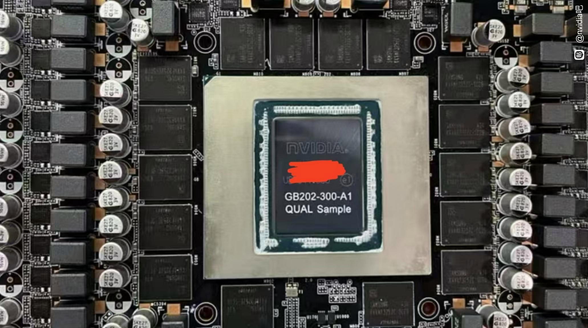
The leaked image flaunts the RTX 5090 in all its glory. The GB202 die powering the RTX 5090 is rumored to be Nvidia’s largest consumer-grade GPU since 2018, at744mm-squared. Some quick measurements fromHarukazesuggest that the GPU package size (including the metallic frame) measures roughly 64mm x 59mm or approximately 3,776 square millimeters.
The reticle limit enables for a maximum chip size of around 850mm-squared assuming our GPU is monolithic. GPUs in that ballpark from Nvidia are typically reserved for data centers; see the B100, H100, A100, and V100 accelerators. Nvidia normally sticks with smaller chips for its mainstream family and the last exception was the RTX 2080 Ti at 754mm-squared and the Nvidia TITAN V at 815mm-squared but that was more geared towards professionals.

Back on topic, the GB202 package is surrounded by a total of 16 VRAM modules, presumably 16Gb28 Gbpsdies from Samsung. This nets us a total of 32GB of memory, which can be upgraded to 48GB should Nvidia employ24Gbmodules in the future.
RTX 5090 QS PCB with GB202-300-A1, GDDR7Same person shared bare PCB last day. VRAM seems Samsung 28Gbps one.https://t.co/IzURv6KnNA pic.twitter.com/JGXDQhEY2QDecember 26, 2024
The RTX 5090 isrumoredto feature 21,760 CUDA cores equating to 170 SMs out of 192 total SMs in the full-fat GB202 configuration. The RTX 5090 thus employs an 88% enabled die which leaves room for a potential RTX 5090 SUPER or Ti/Tie, whatever suits your fancy, later on, but that’s speculation. Apart from that, the remaining Blackwell lineup looks rather less exciting as the core counts for the RTX 5080 drops by over 50% to 84 SMs, theRTX 5070 Tito 70 SMs, and the RTX 5070 to just 48 SMs.
Nvidia is expected to debut Blackwell with the RTX 5090, RTX 5080, and the RTX 5070 family atCESnext month, per a leak fromZotac. We’ll hear more regarding pricing and performance directly from Jensen on January 6.
Get Tom’s Hardware’s best news and in-depth reviews, straight to your inbox.
Hassam Nasir is a die-hard hardware enthusiast with years of experience as a tech editor and writer, focusing on detailed CPU comparisons and general hardware news. When he’s not working, you’ll find him bending tubes for his ever-evolving custom water-loop gaming rig or benchmarking the latest CPUs and GPUs just for fun.
