Imec and ASML announced on Wednesday that they had made the industry’s logic and DRAM structures using ASML’sASML’sroduction Twinscan EXE:5000 EUV lithography tool with a 0.55 numerical aperture, also known asa high-NA litho system. The successful demonstration of high-resolution patterning with the 0.55NA EUV scanner marks an essential milestone in microelectronics production.
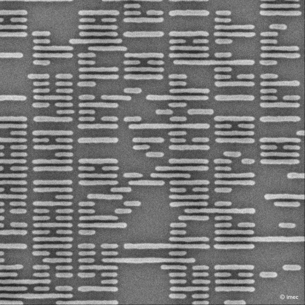
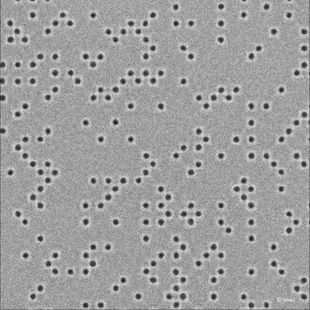
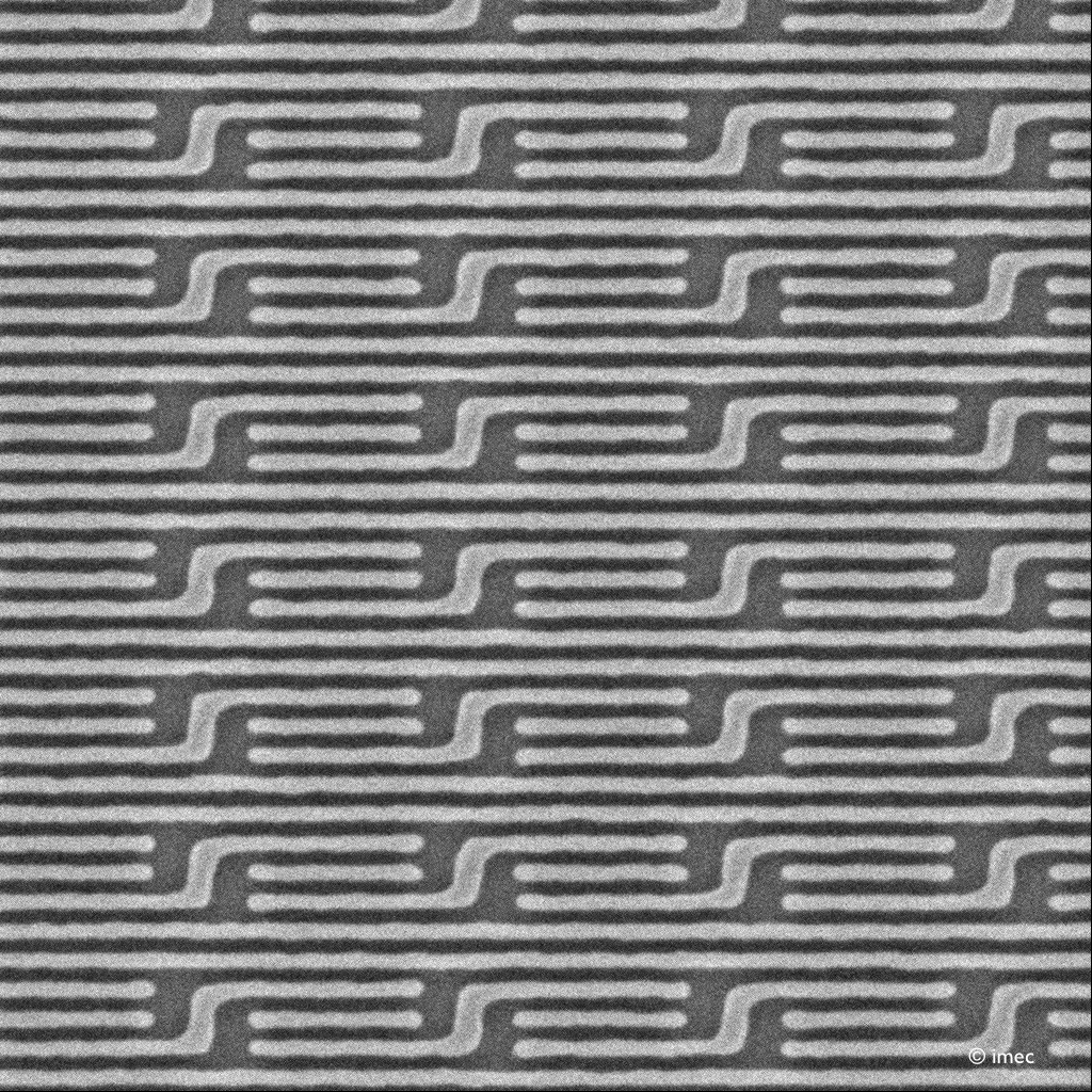
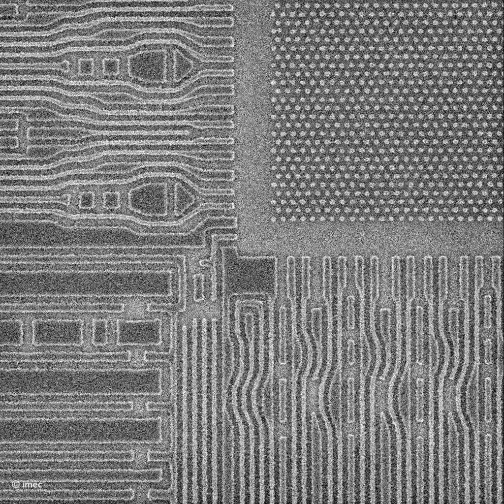
Imec achieved the patterning of random logic structures with 9.5nm dense metal lines (compared to a 13nm resolution in the case of currently used Low-NA tools), which corresponds to a 19nm pitch and a sub 20nm tip-to-tip dimensions, which is good enough to build logic on a 1.4nm-class process technology using a single High-NA exposure. Additionally, Imec successfully created random vias with a 30nm center-to-center distance, showcasing good pattern fidelity and critical dimension uniformity. Furthermore, 2D features were patterned at a 22nm pitch, which is good enough for a 3nm-class fabrication process.
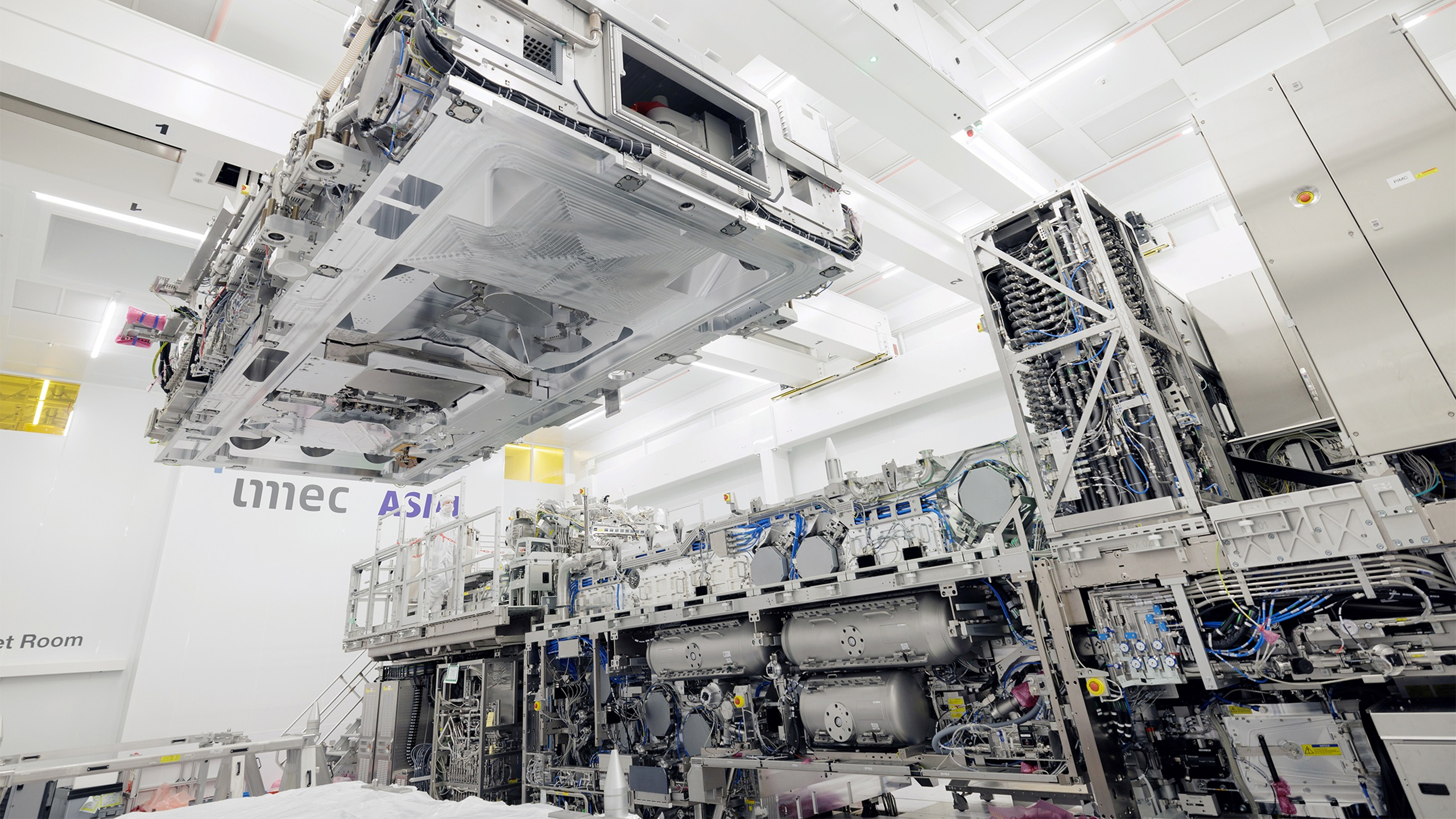
Considering that the pre-production Twinscan EXE High-NA EUV litho system was assembled less than a year ago, the achievements of ASML and Imec at the joint High NA EUV Lithography Lab in Veldhoven, Netherlands, are impressive, to say the least. This follows printing10nm dense lines using high-NA EUVin April.
“The results confirm the long-predicted resolution capability of High NA EUV lithography, targeting sub 20nm pitch metal layers in one single exposure,” said Luc Van den Hove, president and CEO of imec. “High NA EUV will therefore be highly instrumental to continue the dimensional scaling of logic and memory technologies, one of the key pillars to push the roadmaps deep into the ‘angstrom era’. These early demonstrations were only possible thanks to the setup of the joint ASML-imec lab, which allowed our partners to accelerate the introduction of High NA lithography into manufacturing.”
Imec developed pattern designs for DRAM layouts that integrate the storage node landing pad with the bit line periphery at a 32nm pitch in a single exposure. This significant accomplishment underscores High NA technology’s ability to replace several mask layers with a single exposure, simplifying manufacturing processes, shrinking cycle times, and reducing costs.
The success of high-NA EUV patterning is attributed to the optimization of materials and baseline processes by ASML, Imec, and their partners. Preparations involved developing advanced resists, underlayers, and photomasks and transferring High NA EUV baseline processes like optical proximity correction (OPC) and integrated patterning and etch techniques to the 0.55NA EUV scanner.
These results show High NA EUV lithography ecosystem readiness and give ASML customers an idea of how to develop private use cases using the Twinscan EXE:5000 lithography system. Imec plans to provide further insights to support the maturation of High NA EUV-specific materials and equipment, ensuring technology integration into manufacturing processes.
Get Tom’s Hardware’s best news and in-depth reviews, straight to your inbox.
“We are thrilled to demonstrate the world’s first High NA-enabled logic and memory patterning in the joint ASML-imec lab as an initial validation of industry applications,” said Steven Scheer, senior vice president of compute technologies & systems/compute system scaling at imec.
“The results showcase the unique potential for High NA EUV to enable single-print imaging of aggressively-scaled 2D features, improving design flexibility as well as reducing patterning cost and complexity. Looking ahead, we expect to provide valuable insights to our patterning ecosystem partners, supporting them in further maturing High NA EUV specific materials and equipment.”
Anton Shilov is a contributing writer at Tom’s Hardware. Over the past couple of decades, he has covered everything from CPUs and GPUs to supercomputers and from modern process technologies and latest fab tools to high-tech industry trends.