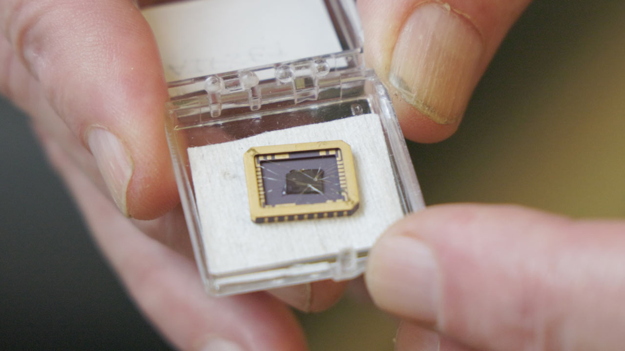
Georgia Tech researchersclaimthey have created “the world’s first functional semiconductor made from graphene.” Importantly, the research team’s epitaxial graphene is claimed to be compatible with conventional microelectronics processing methods and is thus a realistic silicon alternative. Moreover, this refined material achieves a desirable band gap for electronics applications and has latent potential for futurequantum computingdevices.
Technology pundits have highlighted the battle to keepMoore’s Lawalive for years. One of the key issues faced by those wanting to push semiconductors forward is thatsilicon is reaching its limits. Graphene has consistently been touted as awonder material(ever since its discovery in 2004). Still, it has not yet been instrumental to any significant or widely adopted technological breakthrough(s). However, the Georgia Institute of Technology researchers seem to be onto something big with their refined epitaxial graphene bonded to silicon carbide.

To get to this point, Dr. Walter de Heer, Regents’ Professor of Physics at Georgia Tech, led a team of researchers based in Atlanta and Tianjin, China. The professor has been working on 2D graphene since the early 2000s.“We were motivated by the hope of introducing three special properties of graphene into electronics,” he said. “It’s an extremely robust material, one that can handle very large currents, and can do so without heating up and falling apart.”
Despite those three properties, a key semiconductor characteristic has been absent from graphene-based materials until now. “A long-standing problem in graphene electronics is that graphene didn’t have the right band gap and couldn’t switch on and off at the correct ratio,” said Dr. Lei Ma, de Heer’s co-founder of the Tianjin International Center for Nanoparticles and Nanosystems at Tianjin University in China. “Over the years, many have tried to address this with a variety of methods. Our technology achieves the band gap, and is a crucial step in realizing graphene-based electronics.” Lei Ma was also the co-author of theUltrahigh-mobility semiconducting epitaxial graphene on silicon carbidepaper published byNaturetoday.

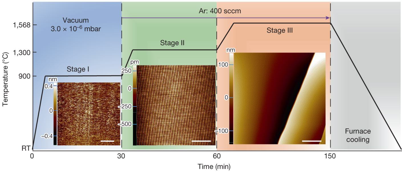
The research team’s breakthrough came as they successfully learned how to grow graphene on silicon carbide wafers using special furnaces – producing epitaxial graphene bonded to silicon carbide. According to the Georgia Tech blog, it took a decade to perfect this material. Now, tests show their graphene-based semiconductor material has ten times greater mobility than silicon. “In other words, the electrons move with very low resistance, which, in electronics, translates to faster computing,” explained the educational and research establishment’s blog.
The Regents' Professor of Physics puts the appealing properties of graphene-based electronics in simpler terms. “It’s like driving on a gravel road versus driving on a freeway,” de Heer said of the electron movement through his refined graphene semiconductor material. “It’s more efficient, it doesn’t heat up as much, and it allows for higher speeds so that the electrons can move faster.”

According to the Georgia Tech research team, their epitaxial graphene bonded to silicon carbide is far superior to any other2D semiconductorsin development. Prof de Heer characterized the semiconductor materials breakthrough as a “Wright brothers moment” and also highlighted the material’s compatibility with the quantum mechanical wave properties of electrons, meaning it could be instrumental to future advances in quantum computing.
Get Tom’s Hardware’s best news and in-depth reviews, straight to your inbox.

Mark Tyson is a news editor at Tom’s Hardware. He enjoys covering the full breadth of PC tech; from business and semiconductor design to products approaching the edge of reason.